
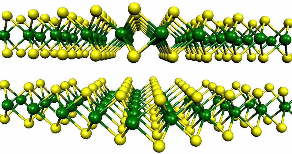

Two-dimensional (2D) layered materials are crystals with strong intralayer bonds but only weak, van-der-Waals type interlayer bonds, such as graphite, MoS2, or hexagonal boron nitride (hBN). They can be exfoliated to an atomically thin monolayer and stacked into heterostructures with almost arbitrary choice ofcombinations. Besides graphene, the most famous 2D materials are transition metal dichalcogenides (TMDCs), specifically MoS2, MoSe2, WS2, and WSe2. These materials have intriguing optical and electronic characteristics. For example, they are indirect semiconductors in the bulk but show strong excitonic emission in the visible range in their monolayer form. We are interested in their optical properties, including exciton-phonon coupling, and in their interactions in heterostructures with other layers.
Projects:
Strong interlayer interactions in two-dimensional pnictogen-based homo- and heterobilayers
Funding source: Deutsche Forschungsgemeinschaft (DFG)
Project leader:

SFB 1719 S04: Exzitonen und Phononen an vertikalen und lateralen Grenzflächen in ultradünnen Halbleitern
Funding source: DFG / Sonderforschungsbereich (SFB)
Acronym: SFB 1719 S04
Project leader:
In project S4,we will investigate the fundamental physicalproperties of novelsolution-grown ultrathin two-dimensional (2D) semiconductors and their verticaland lateral heterostructures by advanced optical spectroscopy. The physicalproperties to be determined include the crystallinestructure and the vibrational, electronic, and optical properties of the 2D semiconductors. In addition, we willexplore the effect of substrate and interfaceinduced strain and the role of defects and grain boundaries o…
Contact Persons:
Participating Scientists:
Publications:
- , , , , :
Two-Dimensional Antimony Oxide
In: Physical Review Letters 124 (2020), p. 126101
ISSN: 0031-9007
DOI: 10.1103/PhysRevLett.124.126101 - , , , :
Phonon dispersion of MoS2
In: Physical Review B 99 (2019), p. 144309
ISSN: 2469-9950
DOI: 10.1103/PhysRevB.99.144309
URL: https://arxiv.org/abs/1809.03381 - , :
Interlayer excitons in MoSe2/WSe2 heterostructures from first principles
In: Physical Review B 97 (2018)
ISSN: 2469-9950
DOI: 10.1103/PhysRevB.97.165306 - , :
Light-Matter Interactions in Two-Dimensional Transition Metal Dichalcogenides: Dominant Excitonic Transitions in Mono- and Few-Layer MoX2 and Band Nesting
In: IEEE Journal of Selected Topics in Quantum Electronics 23 (2017)
ISSN: 1077-260X
DOI: 10.1109/JSTQE.2016.2604359 - , , , :
Interlayer Raman modes in twisted bilayer transition metal dichalcogenides
In: Physical Review B 110 (2024), Article No.: 125431
ISSN: 0163-1829
DOI: 10.1103/PhysRevB.110.125431